Review
. 2017 May 19;17(5):1166.
doi: 10.3390/s17051166.

The Boom in 3D-Printed Sensor Technology

Affiliations
Review

The Boom in 3D-Printed Sensor Technology

Yuanyuan Xu et al. Sensors (Basel). .

Abstract

Future sensing applications will include high-performance features, such as toxin detection, real-time monitoring of physiological events, advanced diagnostics, and connected feedback. However, such multi-functional sensors require advancements in sensitivity, specificity, and throughput with the simultaneous delivery of multiple detection in a short time. Recent advances in 3D printing and electronics have brought us closer to sensors with multiplex advantages, and additive manufacturing approaches offer a new scope for sensor fabrication. To this end, we review the recent advances in 3D-printed cutting-edge sensors. These achievements demonstrate the successful application of 3D-printing technology in sensor fabrication, and the selected studies deeply explore the potential for creating sensors with higher performance. Further development of multi-process 3D printing is expected to expand future sensor utility and availability.

Keywords: 3D printing; additive manufacturing; sensors.


Conflict of interest statement

The authors declare no conflict of interest.

Figures

Figure 1
Figure 1
The process of 3D-printing.
Figure 2
Figure 2
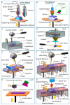
3D printing technologies. (A) Fused deposition modeling (FDM); (B) Directly ink writing (DIW); (C) Stereolithography (SLA); (D) Digital light procession (DLP); (E) Lamination (LOM); (F) Selective laser sintering (SLS) and Selective laser melting (SLM); (G) Photopolymer jetting (Ployjet); (H) Binder jetting(3DP).
Figure 3
Figure 3
(A) Schematic illustration of the embedded 3D-printing process in which conductive ink is printed into an uncured elastomeric reservoir; (B) Photograph of e-3DP for a planar array of soft strain sensors; (C) Top and cross-sectional images (a) of soft sensors, and electrical resistance change as a function of cyclic deformation (b), step deformation (c) and mechanical failure (d); (D) Photograph of a glove with embedded strain sensors (a) produced by e-3DP, electrical resistance changed as a function of time for strain sensors within the glove at five different hand positions (b), and photograph of a three-layer strain and pressure sensor (c). Reproduced from [7], with permission from WILEY-VCH Verlag GmbH & Co. KGaA, Weinheim, Germany, © 2014.
Figure 4
Figure 4
(A) Diagram of different stimuli applied to the PVDF prosthesis; (B) Human ear created with a 3D CAD program (a) and ear prosthesis printed from PVDF (b) and (c); (C) Response of the PVDF prosthesis as a pressure sensor from 0 to 16,350 Pa; (D) Thermal response of PVDF prostheses from 2 °C to 90 °C. Reproduced from [13], with permission by the authors © 2016; licensee MDPI, Basel, Switzerland.
Figure 5
Figure 5
(A) Computer visualization (a) of printed hair, with close view (b) and SEM photo (c) of actual printed hair; (B) Hedgehog with printed hair; (C) Printed hair arrays on curved surfaces; (D) Swiping speed mapped to the gray scale of the block; (E) 2D feature space for rabbit petting labeled using SVM classifier; (F) Direction of swiping on the hairy surface can be differentiated. When one swipes along the hair direction, the bunny turns green; when one swipes against the hair direction, it turns red. Reproduced from [17], with permission from ACM © 2016.
Figure 6
Figure 6
(A) Configuration of the differential transducer with Hall-effect sensors—one magnet system applied in the technology demonstrator: M—micromagnet, A and B—sensors, x—linear displacement, x0—phase shift at maximum sensitivity of Hall sensors; (B) Visualization and (C) design of the sensor; (D) Physical experiments—experimental characteristics of the sensor. Reproduced from [19], with permission from Springer International Publishing AG, Cham, Switzerland © 2016.
Figure 7
Figure 7
(A) CAD and actual fabricated die; (B) Final die with a housing fabricated by traditional manufacturing. Reproduced from [21], with permission from © 2014 IEEE.
Figure 8
Figure 8
(A) Unrolled topology of the stator and rotor silver printed electrodes on flexible foil (Kapton film); (B) Picture of the dismantled sensor; (C) Picture of the assembled sensor. Reproduced from [22], with permission from Advances in Electrical and Computer Engineering © 2016; (D) In-house developed platform (a) and mounted foils and final sensor structure (b); (E) Measured capacitance for the sensor prototype with one full-turn measurement range. Reproduced from [23], with permission from Emerald Group Publishing Limited.
Figure 9
Figure 9
(AD) Electrical characterization of the bionic ear. Reproduced from [25], with permission from the American Chemical Society © 2013; (E) Fabrication steps of acoustic sensor combining 2D inkjet printing and 3D printing techniques; (F) Printed capacitive acoustic transducer; (G) Inkjet printing on thin Mylar film. Reproduced from [26], with permission from by the authors © 2015; licensee MDPI, Basel, Switzerland; (H) The hollow, spherical ceramic shell performing as an ultrasonic transducer. Reproduced from [27], with permission from the authors © 2015, Phys. Status Solidi A, published by WILEY–VCH Verlag GmbH & Co. KGaA, Weinheim, Germany; (I) Designed Near-field monaural localization structure. Reproduced from [28], with permission from by the authors © 2015; licensee MDPI, Basel, Switzerland.
Figure 10
Figure 10
(A) Simulation of the freeform optical sensor illuminating the sample; (B) Photograph of freeform sensor and cylindrical lens array; (C) Freeform optical set up illuminating a metal sample. (D,E) Representation of the splitting and diverging process of freeform optical sensor. Reproduced from [29], with permission from SPIE © 2015; (F) Photograph of the fiber optic vibration sensors. Reproduced from [30], with permission from SPIE © 2016; (G) Drawing of planar optronic sensor system. Reproduced from [31], with permission from Elsevier Ltd. © 2015; (H) User inputs such as push (a), rotation(b), linear movement (c), and acceleration (d) can be sensed by the displacement of a 3D printed light guide. Reproduced from [32], with permission from ACM © 2012.
Figure 11
Figure 11
(A) A 3 × 3 array of the 3D folded loop FSS. Reproduced from [33], with permission from IEEE © 2013; (B) 3D printing to form structures with hollow channels and chambers (a). A finished 3D structure with the injection hole (b). Liquid metal filling (c), and surface planarization to remove the injection hole and extra metal (d). Optical photos of the 3D printed structures (e). Reproduced from [34], with permission from IEEE © 2015; (C) Example of a 3D printed EEG electrode coated with silver paint. Reproduced from [35], with permission from the authors © 2016; licensee MDPI, Basel, Switzerland; (D) A picture of 3D printed object deposited with Ti/Au. Reproduced from [36], with permission from IEEE © 2015; (E) Array of cantilevers (b); The high precision at the interface of the two resins (c); Example of superimposition of optical images acquired for the sample in its initial position (0) and when the magnet approached (d). Reproduced from [38], with permission from the American Chemical Society © 2016.
Figure 12
Figure 12
(A) Photograph of the fabricated transceiver and the sensors (a), a CAD illustration of the transceiver design (b), the measured and expected received return signal strength versus distance using a 43 dBm EIRP transmitter and 11 dBi gain receiver (c). Reproduced from [41], with permission from IEEE © 2015; (B) Schematic illustration of an electrically small antenna with labeled geometric parameters (a) and the optical image of an antenna during the printing process (b), optical profilometry scan of representative meanderlines on electrically small antennas with the background surface subtracted and scanning electron microscopy image of these features (inset). Reproduced from [39], with permission from WILEY-VCH Verlag GmbH & Co. KGaA, Weinheim, Germany, © 2011; (C) Sensor model (a) and completed sensor (b,c). Reproduced from [43], with permission from IEEE © 2014.
Figure 13
Figure 13
Device principle and microscale 3D-printing procedure. (A) In print step 1, a 0.5-μm dextran thin-film sacrificial layer is printed; (B) In print step 2, a 3 μm TPU thin-film cantilever base is printed; (C) In print step 3, a 6.5-μm-thick CB:TPU strain sensor loop is added to the cantilever base; (D) In print step 4, a 1.5-μm TPU wire cover is added; (E) In print step 5, 20-μm-tall, 60-μm-wide PDMS microfilaments are printed in slightly overlapping lines. The filaments constitute the top part of the cantilever and guide cardiomyocytes to form anisotropic laminar tissues; (F) In print step 6, electrical leads and contact are added using a high-conductivity Ag:PA ink; (G) In print step 7, covers to insulate exposed wires and wells to contain cells and media are printed using PDMS, PLA or ABS. Reproduced from [45], with permission from © Macmillan Publishers Limited, part of Springer Nature.
Figure 14
Figure 14
(A) Optical images of the devices (a,b), photograph depicting SPE which is flexible and can be bended easily (c), computational domain of microfluidic cell with the work electrode (d), profile of microfluidic cell from the side view (e). Reproduced from [46], with permission from the American Chemical Society © 2016; (B) Layout of three electrodes: (a) designed device, (b) fabricated device. Reproduced from [47], with permission from Elsevier B.V. © 2012. (C,D) 3D-printed main array and wash reservoir module. Reproduced from [49], with permission from Elsevier B.V. © 2015.
Figure 15
Figure 15
(A) Schematic diagram of the additive 3D manufacturing process. The 3D fabrication process with embedded and electrically conductive structures (a). 3D microelectronics components, including parallel-plate capacitors, solenoid-type inductors, and meandering-shape resistors (b). A 3D LC tank, which is formed by combining a solenoid-type inductor and a parallel-plate capacitor (c). A wireless passive sensor demonstration of a “smart cap,” containing the 3D-printed LC-resonant circuit (d); (B) An optical image of fabricated microelectronics components; (C) The proposed “smart cap” for rapid detection of liquid food quality featuring wireless readout. Reproduced from [50], with permission from Macmillan Publishers Limited, part of Springer Nature © 2017.
Figure 16
Figure 16
(A) 3D printed dog’s nose including a removable PUF insert within the flow path in the vestibule of the nose that collects inspired DNT vapor (a) and schlieren image of the 3D printed dog’s nose during the inspiratory phase of sniffing (b); Reproduced from [51], with permission from ©2017 Macmillan Publishers Limited, part of Springer Nature (B) SEM images of the fabricated sensor with alumina supported bi-metal catalyst deposited on the electrode by screen printing and inkjet printing. Reproduced from [52], with permission from © 2016 Elsevier B.V; (C) Schematic of the 3D printed virtual impactor integrated with QCM sensor for detecting airborne particles; (D) The virtual impactor fabricated by 3D printed technology; (E) Photograph of the experimental setup for prototype characterization. Reproduced from [53], with permission from © 2016 Elsevier B.V.
Figure 17
Figure 17
(A) Sensor architecture showing the primary components of the micro-hair sensor; (B) (left) SEM of 1000 μm long micro-hair structure at 45° tilt (scale bar 200 μm) and (right) surface of the PEDOT: PSS micro-hair (scale bar 10 μm); (C) Cross section of PDMS venturi with gold traces on the disposable sensor substrate; (D) Output from 3-channel sensor filtered and shown over a single cycle (ramp up and down) of sensor operation. Reproduced from [54], with permission from © 2015 IEEE; (E,F) Photograph of the printed flow sensor and impeller. Reproduced from [55], with permission from © 2014 IOP Publishing Ltd.
Figure 18
Figure 18
(A) Schematic representation of a sensing phenomenon of the proposed humidity Sensor; (B) The inkjet-printed sensor’s electrodes with sliver ink. Reproduced from [57], with permission from © 2016 Elsevier Ltd; (C) Optical picture of the inkjet-printed capacitors and resistor on paper. Reproduced from [58], with permission from © 2011 IEEE; (D) Overhead view of the continuous sensor (black) on a carbon substrate (a), and thermal image produced by EIT formed upon cooling the center of the continuous sensor from 68.5 °C (red) to 7 °C (blue) using a Peltier element. Reproduced from [59], with permission from © 2015 WILEY-VCH Verlag GmbH & Co. KGaA, Weinheim; (E) Photograph of an IC 7400N prepared for DLW (a), Scanning electron micrograph (SEM) of temperature probes on the chip surface (b), SEM showing a close-up of temperature probes colored in green (c), scheme of the three probe positions on the chip on which measurements have been performed (d), the temperature measured at the three probe positions and DC of the applied voltage (e). Reproduced from [60], with permission from © 2015 AIP Publishing LLC.

Similar articles

Cited by

References

    1. MacDonald E., Wicker R. Multiprocess 3D printing for increasing component functionality. Science. 2016;353 doi: 10.1126/science.aaf2093. - DOI - PubMed
    1. Rim Y.S., Bae S.-H., Chen H., de Marco N., Yang Y. Recent Progress in Materials and Devices toward Printable and Flexible Sensors. Adv. Mater. 2016;28:4415–4440. doi: 10.1002/adma.201505118. - DOI - PubMed
    1. Garnier F., Hajlaoui R., Yassar A., Srivastava P. All-Polymer Field-Effect Transistor Realized byPrinting Techniques. Science. 1994;265:1684–1686. doi: 10.1126/science.265.5179.1684. - DOI - PubMed
    1. Bao Z., Feng Y., Dodabalapur A., Raju V.R., Lovinger A.J. High-Performance Plastic Transistors Fabricated by Printing Techniques. Chem. Mater. 1997;9:1299–1301. doi: 10.1021/cm9701163. - DOI
    1. Ridley B.A., Nivi B., Jacobson J.M. All-Inorganic Field Effect Transistors Fabricated by Printing. Science. 1999;286:746–749. doi: 10.1126/science.286.5440.746. - DOI - PubMed
  NODES
INTERN 1
twitter 2