Review
. 2021 Aug 28;24(9):103050.
doi: 10.1016/j.isci.2021.103050. eCollection 2021 Sep 24.

Unconventional van der Waals heterostructures beyond stacking

Affiliations
Review

Unconventional van der Waals heterostructures beyond stacking

Peter Sutter et al. iScience. .

Abstract

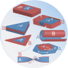
Two-dimensional crystals provide exceptional opportunities for integrating dissimilar materials and forming interfaces where distinct properties and phenomena emerge. To date, research has focused on two basic heterostructure types: vertical van der Waals stacks and laterally joined monolayer crystals with in-plane line interfaces. Much more diverse architectures and interface configurations can be realized in the few-layer and multilayer regime, and if mechanical stacking and single-layer growth are replaced by processes taking advantage of self-organization, conversions between polymorphs, phase separation, strain effects, and shaping into the third dimension. Here, we highlight such opportunities for engineering heterostructures, focusing on group IV chalcogenides, a class of layered semiconductors that lend themselves exceptionally well for exploring novel van der Waals architectures, as well as advanced methods including in situ microscopy during growth and nanometer-scale probes of light-matter interactions. The chosen examples point to fruitful future directions and inspire innovative developments to create unconventional van der Waals heterostructures beyond stacking.

Keywords: materials synthesis; nanotechnology; nanotechnology fabrication.


Conflict of interest statement

The authors declare no competing interests.

Figures
None
Graphical abstract
Figure 1
Figure 1
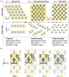
Van der Waals crystals for unconventional heterostructures (A) Structurally diverse Sn sulfides as building blocks for van der Waals heterostructures. Stable bulk crystals include the dichalcogenide SnS2 and monochalcogenide SnS, as well as a Sn2S3 structure with intermediate stoichiometry and mixed Sn(II)/Sn(IV) cation valence. (B) Anisotropic group IV monochalcogenides. Isostructural layered crystals with stoichiometry MX (M: Ge, Sn; X: S, Se) provide opportunities for integration of materials with anisotropic lattice mismatch and properties. Rectangles outline the in-plane unit cells of the different orthorhombic MX crystals. Relaxed lattice parameters along the a and b crystal axes represent values computed by density functional theory (Jain et al., 2013).
Figure 2
Figure 2
In situ microscopy of growth and transformations of 2D crystals and heterostructures (A) Scanning transmission electron microscopy (STEM) provides atomic-resolution imaging at high temperatures, as illustrated by dynamic observations of evolving edge reconstructions of Mo0.95W0.05 Se2 monolayers at 500°C. Adapted from Sang et al. (2018). Copyright 2018 Springer Nature. (B) Environmental scanning electron microscopy (SEM) provides mesoscale imaging during 2D/layered crystal growth at high temperatures and during exposure to gases or vapors, as illustrated by observations of graphene growth on Cu foils at 1000°C. Scale bar: 5 μm. Adapted from Wang et al. (2015). Copyright 2015 American Chemical Society. (C) Low-energy electron microscopy (LEEM) enables real-time microscopy of growth and processing of 2D/layered crystals and heterostructures during exposure to vapors or gases at high temperature, as illustrated by the observation of macroscopic graphene growth on Ru(0001) at 850°C. Adapted from Sutter et al. (2008). Copyright 2008 Springer Nature.
Figure 3
Figure 3
Sub-diffraction optoelectronics and photonics in van der Waals crystals and heterostructures. (A and B) Aperture SNOM. (A) Efficient bidirectional coupling between macroscopic and nanometer length scales in shaped plasmonic SNOM probes. Adapted from Bao et al. (2012). Copyright 2012 American Association for the Advancement of Science. (B) Luminescence mapping of a single-layer MoS2 flake shows nanoscale heterogeneity at the flake edges and locally in the interior. Adapted from Bao et al. (2015). Copyright 2015 Springer Nature. (C and D) Scattering SNOM. (C) Schematic of a setup for nano-infrared (IR) imaging of plasmon polaritons in twisted bilayer graphene. (D) Nano-IR amplitude image for a plasmon polariton wavelength λp = 135 nm, demonstrating the periodic variations in the optical response arising from the modification of the electronic structures at moiré domain walls (solitons) in rotationally misaligned graphene layers. Adapted from Sunku et al. (2018). Copyright 2018 American Association for the Advancement of Science. (E-G) Nano-optoelectronics in scanning transmission electron microscopy (STEM). (E) Schematic of cathodoluminescence (CL) and electron energy-loss spectroscopy (EELS), two major types of electron beam excitation and detection suitable for probing optoelectronics and photonics at the nanoscale. (F) Local absorption measurements using monochromated EELS in MoS2 and MoSe2 parts of a heterogeneous MoS2xSe2(1-x) monolayer, compared with a spatially averaged photoluminescence spectrum of the same sample. Adapted from Tizei et al. (2015). Copyright 2015 American Physical Society. (G) Schematic and STEM image of a lateral heterostructure between multilayer SnS and GeS (top); hyperspectral CL linescan and corresponding STEM intensity profile across the lateral GeS-SnS interface (bottom). Adapted from Sutter et al. (2020a). Copyright 2020 American Chemical Society.
Figure 4
Figure 4
Tin chalcogenide heterostructures via phase conversion (A–D) Electron-beam-induced transformation of SnS2 into SnS suspended in a SnS2 matrix. (A) Schematic of the electron-beam-induced (knock-on) generation of S vacancies. (B) EDS spectra documenting the change in composition from SnS2 to SnS, (1)–(2), followed by a global signal reduction indicating thinning by the electron beam, (2)–(3). (C) TEM images and electron diffraction patterns obtained during the electron beam-induced SnS2 to SnS transformation. (D) Thickness-dependence of the final SnS morphologies after the transformation. Adapted from Sutter et al. (2016). Copyright 2016 American Chemical Society. (E–G) Bottom-up synthesis of twisted chalcogenides. (E) Comparison of ordinary van der Waals epitaxy and of a two-step process yielding twisted layer stacks. (F) In situ LEEM of the spontaneous formation of 30°-twisted t-SnS2 by growth and transformation of azimuthally aligned SnS on an SnS2 substrate. (G) Phase identification by local low-energy electron diffraction (micro-LEED): SnS2 substrate (blue); SnS azimuthally aligned with the SnS2 substrate, where (11)SnS(10)SnS2 (red); and 30°-twisted t-SnS2 (green). Adapted from Sutter et al. (2019c). Copyright 2019 Springer Nature.
Figure 5
Figure 5
Wrap-around core–shell heterostructures via spontaneous phase separation of structurally incompatible van der Waals crystals (A) Schematic of SnS–SnS2 wrap-around core-shell heterostructures formed during SnS growth with a small excess of sulfur. The core-shell geometry involves two-types of van der Waals interfaces, with IFcorresponding to ordinary van der Waals stacking along the top and bottom facets while IF along the side facets consists of orthogonal core and shell layering. (B) High-resolution TEM near the core-shell interface, showing the layered SnS2 shell tightly enclosing the SnS core. M: Moiré structure due to superposition of the lattices of the SnS core and of the crystalline SnS2 shell. (C) Tauc plot obtained by UV-Vis absorption on a dense array of wrap-around core-shell flakes, showing two distinct absorption onsets at 1.20 eV and 0.65 eV, respectively. (D) STEM image of a SnS–SnS2 wrap-around core-shell structure. Axes identify the SnS lattice directions. (E) Hyperspectral CL linescan along the arrow in D, showing luminescence quenching near the IF core-shell interface. (F) Band diagram illustrating the type II band offset (responsible for charge separation, dashed arrow), band-to-band absorption in SnS, and interfacial (spatially indirect) absorption at the core-shell interface. Adapted from Sutter et al. (2019d). Copyright 2019 Wiley-VCH.
Figure 6
Figure 6
3D architectures of 2D/layered crystals (A and B) Shape tuning and self-folding using stimuli-responsive actuators. (A) Solvent-induced self-actuation of graphene membranes using differentially cross-linked films of an SU8 negative epoxy. Adapted from Huang et al. (2020). Copyright 2020 Wiley-VCH. (B) Reversible self-folding of a box made of graphene paper, actuated by near-infrared (NIR) light exposure (On: with NIR light; Off: without NIR light). Adapted from Mu et al. (2015). Copyright 2015 American Association for the Advancement of Science. (C) Graphene kirigami for stretchable graphene electronics. Top: Paper model; Bottom: Graphene spring stretched by ∼70% from its rest length. Adapted from Blees et al. (2015). Copyright 2015 Springer Nature. (D and E) Scrolls of 2D crystals and heterostacks. (D) Self-rolled-up 3D graphene field-effect transistor (GFET) photodetector, using a combination of compressively strained and tensile strained SiNx support layers and a sacrificial Al release layer. Adapted from Deng et al. (2019). Copyright 2019 American Chemical Society. (E) High-order superlattices of van der Waals heterostructures spontaneously generated by delamination via liquid intercalation at the interface to the substrate and a capillary force induced spontaneous rolling process. Adapted from Zhao et al. (2021). Copyright 2021 Springer Nature. (F) Spontaneous twisting of chalcogenide nanoribbons. Ge1-xSnxS alloy nanoribbons with SnS enriched edges, synthesized by Au-catalyzed vapor-liquid-solid growth show spontaneous axial twisting, thus generating 3D waveguides with continuously varying orientation. CL measurements show excitation of traveling TE0 photonic modes by a focused electron beam exclusively in vertical section of the nanoribbon waveguides, where the electrons propagate parallel to the ribbon plane. Adapted from Sutter et al. (2021b). Copyright 2020 Wiley-VCH.

Similar articles

Cited by

References

    1. Agnoli S., Granozzi G. Second generation graphene: opportunities and challenges for surface science. Surf. Sci. 2013;609:1–5. doi: 10.1016/j.susc.2012.11.016. - DOI
    1. Ahn S.J., Moon P., Kim T.-H., Kim H.-W., Shin H.-C., Kim E.H., Cha H.W., Kahng S.-J., Kim P., Koshino M. Dirac electrons in a dodecagonal graphene quasicrystal. Science. 2018;361:782–786. doi: 10.1126/science.aar8412. - DOI - PubMed
    1. Bai Y., Yue H., Wang J., Shen B., Sun S., Wang S., Wang H., Li X., Xu Z., Zhang R., Wei F. Super-durable ultralong carbon nanotubes. Science. 2020;369:1104–1106. doi: 10.1126/science.aay5220. - DOI - PubMed
    1. Bao W., Borys N.J., Ko C., Suh J., Fan W., Thron A., Zhang Y., Buyanin A., Zhang J., Cabrini S. Visualizing nanoscale excitonic relaxation properties of disordered edges and grain boundaries in monolayer molybdenum disulfide. Nat. Commun. 2015;6:7993. doi: 10.1038/ncomms8993. - DOI - PMC - PubMed
    1. Bao W., Melli M., Caselli N., Riboli F., Wiersma D.S., Staffaroni M., Choo H., Ogletree D.F., Aloni S., Bokor J. Mapping local charge recombination heterogeneity by multidimensional nanospectroscopic imaging. Science. 2012;338:1317–1321. doi: 10.1126/science.1227977. - DOI - PubMed

LinkOut - more resources

  NODES
Association 3
Note 2
twitter 2